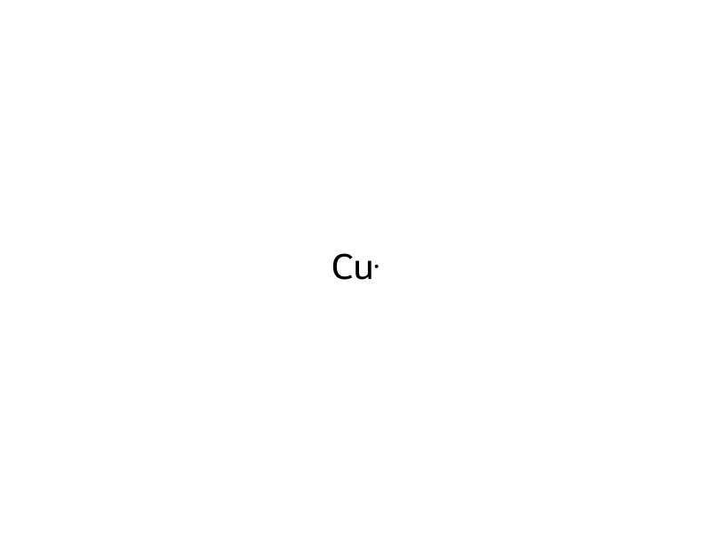
Copper → Cupric chromate(VI)
Reaction equation

[Cu:1].[Cr:2]([O-:6])([O-:5])(=[O:4])=[O:3].[Cr:7]([O-:10])([O-:9])=[O:8]>>[Cr:2]([O-:6])([O-:5])(=[O:4])=[O:3].[Cu+2:1].[Cr:7]([O-:10])([O-:9])=[O:8].[Cu+2:1]Participants


Procedure
A passivating film 46 is then formed on top of the deposited copper layer 44 by depositing one of either a chromate or chromite on the deposited copper layer and forming a respective copper chromate or copper chromite composition. The passivating layer deposition could be formed by passing the wafer through a heating oven and depositing the chromite or chromate onto the deposited copper layer 44. It is also possible to use other techniques, even a wet technique. The semiconductor wafer and associated layers are then passed to a mechanical tool 48 for performing chemical mechanical polishing on the wafer 31. The wafer 31 is carried by wafer carrier 49 and placed face-down on a polishing pad 50 so that the wafer surface to be polished rests against the surface of the polishing pad 50. Various drive mechanisms 52 provide the rotation and movement of a wafer 31 relative to the polishing pad 50. The polishing pad can rotate in operation.
Sources & evidence
- ORD record
- ord-424bd4d6313544a4ad8166710d14656a
- Source dataset
- uspto-grants-2000_09
- Patent number
- US06114234
Reaction notes
Loading…